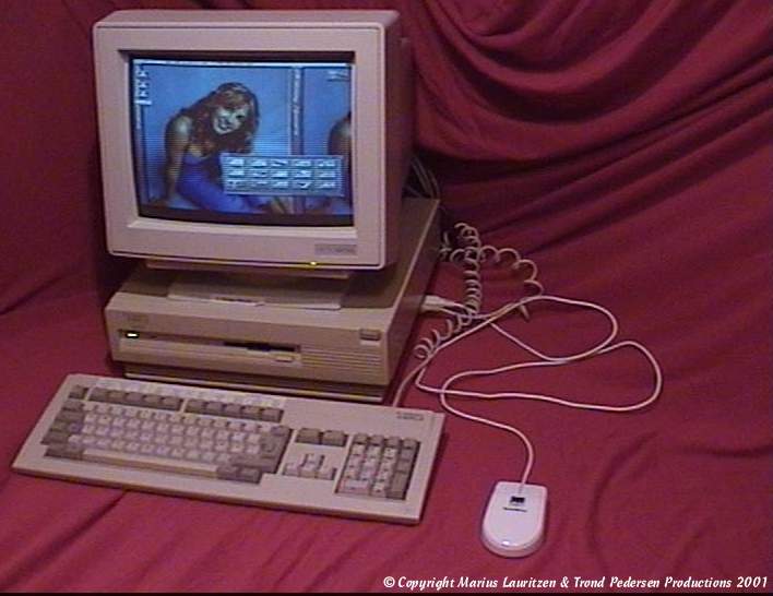

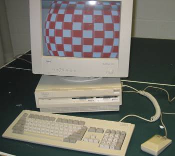
A3000 with twin floppy drives.
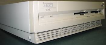
Picture showing the front of the A3000
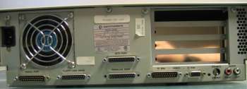
Picture showing the rear of the A3000
Hi Res Version of A3000 with twin floppy drives (1900 x 1704)
Hi Res Version of A3000 Front (2000 x 868)
Hi Res Version of A3000 Rear (2000 x 724)
Picture of US A3000 Keyboard (2000 x 950)
Picture of Rev 6.1 Motherboard (596 x 636) (030@25Mhz, 68882, 1MB Chip, DMAC & ROMs missing)
Picture of Rev 6.x Motherboard (582 x 600)
Picture of Rev 8.0 Motherboard (622 x 652) (030@25Mhz, 68882, 1MB Fast, 1MB Chip)
Picture of Rev 8.9 Motherboard (626 x 666) (030@25Mhz, 68882, 1MB Fast, 1MB Chip)
Picture of Rev 9.0 Motherboard (1728 x 1704) (030@25Mhz, 68882)
Picture of Rev 5.0 Daughterboard (593 x 198)
Picture of Rev 9.0 Daughterboard (598 x 204)
Picture of a ROM Tower
French article on hacking the FPU to 50Mhz
Standard Specifications
| Case Type: | Desktop |
| Processor: | 030@16Mhz or 030@25Mhz |
| MMU: | Internal |
| FPU: | 68881@16Mhz (for 030@16Mhz version) 68882@25Mhz (for 030@25Mhz version) |
| Chipset: | ECS (Plus additional chips such as Amber, SuperDMAC and Ramsey) |
| Kickstarts: | V1.4 (Special Kickstart versions which boots the real Kickstart from a file called dev:kickstart) V2.04 (in ROM, or disk based for Kickstart V1.4) |
| Bus Controller: | Fat Buster Rev 2 Super Buster Rev 6 Super Buster Rev 7 Super Buster Rev 9 Super Buster Rev 11 (unconfirmed) |
| Expansion Slots: | 4 x 100pin Zorro III slots 1 x ECS Video Slot (inline with Zorro) 2 x Inactive 16bit ISA slots (inline with Zorro) 1 x 200pin CPU Fast Slot. |
| Standard CHIP RAM: | 1MB |
| RAM sockets: | 44256 DRAM DIP Sockets for Chip RAM (Max 2MB) ZIP sockets and DIP sockets for fast RAM |
| Hard Drive Controllers: | 1 x SCSI-II controller |
| Drive Bays: | 3 x 3.5" Drivebays (2 with faceplates, these are fixed as part of the A3000 case) |
| Expansion Ports: | 1 x 25pin Serial 1 x 25pin Parallel 1 x 23pin RGB Video 1 x 15pin VGA 1 x 23pin External Floppy 2 x 9pin Joystick/Mouse 2 x RCA Audio (Left/Right) 1 x 25pin SCSI Connector 1 x large 5pin DIN Keyboard connector |
| Floppy Drive: | 1 x Internal 880K Floppy Drive or 1 x Internal 1.76MB Floppy Drive |
| Motherboard Revisions: | Rev 6.0 (pre-production) Rev 6.1 (First production release) Rev 7.1 (Used ROM tower) Rev 7.2 Rev 7.3 Rev 8.0 Rev 8.9 Rev 9.0 (no ROM Tower, jumpers are labelled) |
| Battery Backed Up Clock: | Yes, uses "Barrel" shaped battery. |
The A3000 is regarded by some Amiga fans as the best model ever made, but they generally forget about the A3000T and A4000T which actually offer a lot more. The A3000 unlike most Amiga models, supports both ROM based Kickstarts and disk based Kickstarts, although not simultaneously. Kickstart V1.4 is actually a special version of Kickstart which loads the real Kickstart from a file called DEVS:Kickstart. Kickstart V2.04 was available as a ROM, or as a disk based version for use with A3000's which had Kickstart V1.4. A3000's fitted with Kickstart V1.4 cannot use 040 or 060 processors, regardless of what version of Kickstart is eventually booted, because it relies heavily in the integrated MMU in the 030 which varies to some degree from the MMU in 040 and 060 processors. The A3000 also contains a built in scandoubler and flicker fixer so that standard PC type SVGA monitors can be connected and display the native (PAL/NTSC) screen modes and was available as a separate card for other Amigas called the A2320. The scandoubler can be disabled if necessary by a switch on the back of the machine. There is also a variable switch to finetune the scandoubler .The A3000 has a SCSI-II controller (WDC33C93) on the motherboard which is much faster than the standard IDE Controller that was supplied with the A4000 and other models. However some motherboard revisions have SCSI termination directly on the motherboard and others don't. You may find you need at least one SCSI device attached in order to boot, even from floppy disk. The A3000 is one of the few models of Amigas which actually has some NVRAM, primarily for storing the configuration settings of the SCSI controller, such as Controller ID, SCSI bus timeout, Synchronous mode and LUNs.
There are RAM sockets on the motherboard for expanding CHIP RAM up to 2MB, providing your Agnus chip supports it. These are in the form of DIP sockets. The motherboard also contains 32 ZIP CHIP sockets and 20 DIP sockets for adding additional memory. If the DIP sockets are used then only a maximum of 4MB of Fast RAM can be added. If ZIP memory is used then 16MB of Fast RAM can be added. The ZIP and DIP sockets cannot be used simultaneously. If you intend to use Zorro III cards which make use of Zorro III DMA then you need to upgrade Buster to Rev 11. The Zorro III and ISA expansion slots are on a daughterboard (riser card) which is connected to the motherboard and rises vertically from it.
Motherboard Layout
Jumpers
| JUMPER | PINS | 16MHz PAL 313311-01 |
16 MHz NTSC 313311-02 |
25 MHz PAL 313311-03 |
25 MHz NTSC 313311-04 |
FUNCTION |
|---|---|---|---|---|---|---|
| J100 | 4 | 2-3 | 2-3 | 1-2 | 1-2 | QUADCLK (Quadrature Clock Source) |
| J101 | 3 | 2-3 | 2-3 | 2-3 | 2-3 | FPU Clock Source |
| J102 | 3 | 2-3 | 2-3 | 2-3 | 2-3 | BRDCLK (System Clock Source) |
| J103 | 4 | 3-4 | 3-4 | 3-4 | 3-4 | FPU CS/BERR |
| J104 | 3 | 1-2 | 1-2 | 1-2 | 1-2 | CPUCLK (CPU Clock Source) |
| J151 | 3 | 2-3 | 2-3 | 1-2 | 1-2 | ROM Timing |
| J152 | 3 | 2-3 | 2-3 | 1-2 | 1-2 | ROM Timing |
| J180 | 3 | 2-3 | 2-3 | 2-3 | 2-3 | A2000 ROM Compatibility Jumpers |
| J181 | 3 | 2-3 | 2-3 | 2-3 | 2-3 | A2000 ROM Compatibility Jumpers |
| J200 | 3 | 1-2 | 2-3 | 1-2 | 2-3 | NTSC/PAL Select |
| J350 | 3 | 1-2 | 1-2 | 1-2 | 1-2 | Tick Clock Source |
| J351 | 3 | 2-3 | 2-3 | 2-3 | 2-3 | Disable DF1: (1-2 enable) |
| J352 | 2-3 | 2-3 | 2-3 | 2-3 | Light Pen Source | |
| J481 | 3 | 2-3 | 2-3 | 2-3 | 2-3 | VDE Scan Double Only Jumper |
| J482 | 3 | 1-2 | 1-2 | 1-2 | 1-2 | VDE PLL Loop Adjust |
| J483 | 3 | - | - | - | - | VDE Factory Test Points |
| J800 | 3 | 1-2 | 1-2 | 1-2 | 1-2 | WD33C93 |
| J851 | 3 | 1-2 | 1-2 | 2-3 | 2-3 | RAM Controller Speed Jumper |
| J852 | 5 | 4-5 | 4-5 | 4-5 | 4-5 | -012A Ramsey Only (See Notes) J852 connecting pins 2 & 3 : 1Mbit, in 256k x 4 J852 connecting pins 1 & 2 : 4Mbit, in 1m x 4 |
| J853 | 3 | 2-3 | 2-3 | 2-3 | 2-3 | -012A Ramsey Only (See Notes) |
Notes:
J150, J151: ROM Timing.
The ROM timing circuit provides four different speed settings to match the output enable and access timing of the system ROMs. To set the jumpers, determine the output enable time and access times for the ROMs you wish to use. The ROM must have lower values than the setting you select. System standard ROMs have T(oe) = 110ns and T(acc) = 250ns.
| CLOCK | J151 | J150 | T(oe)(min) | T(acc)(min) |
|---|---|---|---|---|
| 16Mhz | 2-3 | 2-3 | 157ns | 250ns |
| 16Mhz | 2-3 | 1-2 | 220ns | 312ns |
| 16Mhz | 1-2 | 2-3 | 282ns | 375ns |
| 16Mhz | 1-2 | 1-2 | 345ns | 437ns |
| 25Mhz | 2-3 | 2-3 | 90ns | 160ns |
| 25Mhz | 2-3 | 1-2 | 130ns | 200ns |
| 25Mhz | 1-2 | 2-3 | 170ns | 240ns |
| 25Mhz | 1-2 | 1-2 | 210ns | 280ns |
| J180 | J181 | |
|---|---|---|
| A2000/A500 ROMS | 1-2 | 1-2 |
| A3000 ROMS | 2-3 | 2-3 |
| J852 | J853 | |
|---|---|---|
| -012A Ramsey w/ 256K4 RAMs | 4-5 | 2-3 |
| Later Ramseys w/ 256K4 RAMs | 2-3 | 1-2 |
| Later Ramseys w/ 1M4 RAMs | 1-2 | 1-2 |
Thanks to Rick Harris, Ron Mascaro, Greg Scott, Dave Haynie, Erik Wallen, Marius Lauritzen, Orjan Lindgren and NicDouille