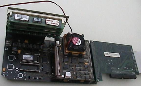
Cyberstorm showing all the modules connected.
Cyberstorm showing all the modules connected.
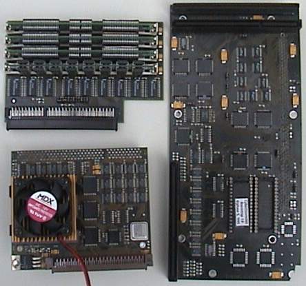
Cyberstorm with individual modules
| Processor: | 040@25Mhz, 040@40Mhz or 060@50Mhz |
| FPU: | Internal |
| MMU: | Internal |
| Max Ram: | 128MB |
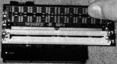
| Ram Type: | 4 x 72pin SIMM slots. |
The Cyberstorm Mk-I is of a modular design and comes in three main parts (4 if you include SCSI II). The main part called the carrier board actually connects into the processor slot on the motherboard. The next component is referred to as the processor daughterboard. This is a small card which contains either an 040@25Mhz, 040@40Mhz or an 060@50Mhz, and usually contains a heat sink and/or fan. The processor daughterboard connects on top of the carrier board in parallel. The third component is the memory daughterboard. This contains 4 x 72pin SIMM slots for adding up to a maximum of 128MB and supports SIMM sizes of 4MB to 32MB in mixed configurations. The memory daughterboard is fitted to the carrier board on top but at right angles. If no memory is intended to be added to the memory daughterboard then it does not have to be fitted. It may not be possible to physically fit this card in a standard A3000 desktop and it may also be necessary to perform an INT-2 modifcation, but this has not been confirmed. If you have the SCSI-II module attached, it may conflict with the internal SCSI controller in an A3000 series machine.
Jumper Settings
For an 040@25Mhz, the jumper marked INT on the A4000 motherboard needs to be set for the Internal Clock Signal. For an 040@40Mhz and 060@50Mhz the jumper needs to be set to EXT for an external Clock Signal.
Main Jumpers
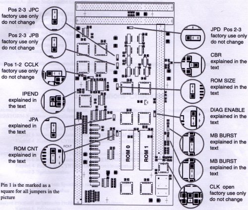
| Jumper Name | Position | Function |
|---|---|---|
| IPEND | ON | No mainboard CPU |
| CBR | ON | CPU on mainboard |
| DIAG | Pos 1-2 | Enable Diagnostic ROM |
| Pos 2-3 | Disable Diagnostic ROM | |
| ROM Size | Pos 1-2 | 16bit ROMs |
| Pos 2-3 | 8bit ROMs | |
| ROM Count | Pos 1-2 | Two ROMs Installed |
| Pos 2-3 | One ROM Installed | |
| JPA | Pos 1-2 | Normal RAM Access |
| Pos 2-3 | Fast RAM Access | |
| OPEN | Slow RAM Access | |
| MB Burst | Pos 1-2 | Enable MainBoard burst access |
| Pos 2-3 | Disable MainBoard burst access |
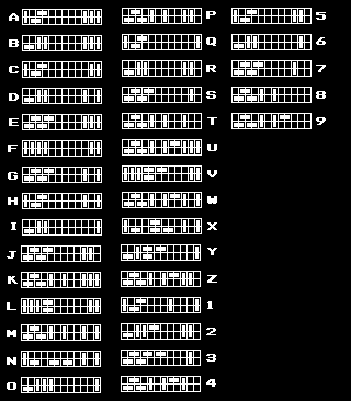
RAM Jumpers
| Total RAM | Bank 0 | Bank 1 | Bank 2 | Bank 3 | Jumper Reference See Diagram Below |
|---|---|---|---|---|---|
| 4/8/12/16MB | 4/0MB | 4/0MB | 4/0MB | 4/0MB | A |
| 8/12/16/20MB | 8MB | 4/0MB | 4/0MB | 4/0MB | B |
| 16/20/24/28MB | 16MB | 4/0MB | 4/0MB | 4/0MB | C |
| 32/36/40/44MB | 32MB | 4/0MB | 4/0MB | 4/0MB | D |
| 16/20/24MB | 8MB | 8MB | 4/0MB | 4/0MB | E |
| 24/28/32MB | 16MB | 8MB | 4/0MB | 4/0MB | F |
| 40/44/48MB | 32MB | 8MB | 4/0MB | 4/0MB | G |
| 32/36/40MB | 16MB | 16MB | 4/0MB | 4/0MB | H |
| 48/52/56MB | 32MB | 16MB | 4/0 | 4/0 | I |
| 64/68/72MB | 32MB | 32MB | 4/0MB | 4/0MB | J |
| 24/28MB | 8MB | 8MB | 8MB | 4/0MB | K |
| 32/36MB | 16MB | 8MB | 8MB | 4/0MB | L |
| 48/52MB | 32MB | 8MB | 8MB | 4/0MB | M |
| 40/44MB | 16MB | 8MB | 8MB | 4/0MB | N |
| 56/60MB | 32MB | 16MB | 8MB | 4/0MB | O |
| 72/76MB | 32MB | 32MB | 8MB | 4/0MB | P |
| 48/52MB | 16MB | 16MB | 16MB | 4/0MB | Q |
| 64/68MB | 32MB | 16MB | 16MB | 4/0MB | R |
| 80/84MB | 32MB | 32MB | 16MB | 4/0MB | S |
| 96/100MB | 32MB | 32MB | 32MB | 4/0 | T |
| 32MB | 8MB | 8MB | 8MB | 8MB | U |
| 40MB | 16MB | 8MB | 8MB | 8MB | V |
| 56MB | 32MB | 8MB | 8MB | 8MB | W |
| 48MB | 16MB | 16MB | 8MB | 8MB | X |
| 64MB | 32MB | 16MB | 8MB | 8MB | Y |
| 80MB | 32MB | 32MB | 8MB | 8MB | Z |
| 56MB | 16MB | 16MB | 16MB | 8MB | 1 |
| 72MB | 32MB | 16MB | 16MB | 8MB | 2 |
| 88MB | 32MB | 32MB | 16MB | 8MB | 3 |
| 104MB | 32MB | 32MB | 32MB | 8MB | 4 |
| 64MB | 16MB | 16MB | 16MB | 16MB | 5 |
| 80MB | 32MB | 16MB | 16MB | 16MB | 6 |
| 96MB | 32MB | 32MB | 16MB | 16MB | 7 |
| 112MB | 32MB | 32MB | 32MB | 16MB | 8 |
| 128MB | 32MB | 32MB | 32MB | 32MB | 9 |
Bank 0 is closest to the connector. The largest SIMM must always be placed in bank 0, with the second largest in bank 1 and so on.
Thanks to Antoine Dubourg